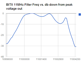
As reported yesterday I have the 20 meter receiver portion of my BITX 20/40 rig up and running. I decided to take a closer look at the crystal filter I built.
Here is my method:
1) Using an Arduino/DDS sig generator, I put 11 Mhz energy into the base of Q2 (the stage immediately prior to the crystal filter).
2) Using my Rigol 1052E oscilloscope, I measured RMS voltage at the output of Q3/Q3A (the stage immediately following the filter).
3) I looked at Vrms as I MANUALLY varied the input frequency in 100 Hz increments.
4) I took the results and plugged them into a spreadsheet. I then used the spreadsheet to calculate the db drop from the peak Vrms value (So I wasn't looking at insertion loss, just the filter shape).
I used 20*LOG(Vrms/276)
5) I ended up with the chart displayed above.
I have a few questions:
1) What do you folks think about my methodology for evaluating the filter?
2) Where would you guys put the BFO frequency?
3) I know the ripple looks ugly, but the receiver sounds great. Should I attempt to get rid of the ripple?
Here is the filter I used (as prescribed by the AADE software): I estimated Q at 10000 and used LM and CM values derived by the G3UUR method, and made no effort to match impedances going into the filter:
Here is what GPLA predicted. I estimated Rin and Rout values. That probably accounts for the difference between the GPLA prediction and what I measured.
Our book: "SolderSmoke -- Global Adventures in Wireless Electronics" http://soldersmoke.com/book.htm Our coffee mugs, T-Shirts, bumper stickers: http://www.cafepress.com/SolderSmoke Our Book Store: http://astore.amazon.com/contracross-20


On crystal/ceramic filters, excessive ripple is a common result from mistermination of the input/output, so it is very possible that your filter is flatter than your sweep indicated.
ReplyDeleteIf you re-sweep your filter, I'd use a resistor in series with your input signal source and a shunt resistor on the output - remembering to put a 47-56 ohm resistor directly on the DDS to keep it loaded. (That wouldn't likely matter over a very narrow frequency range, however. Remember that the 'scope probe has some capacitance, too! (You might need some shunt capacitance on the input, too if your design calls for that in your source impedance.)
Another way to check the filter would be to use a program like Spectran or Spectrum Lab, set it to a large number of averages, and then use it to listen to the noise from the receiver - which should be the shape of the filter plus effects of the audio stages. To make this work, though, you need to be receiving white noise of a high enough level to exceed the noise floor of the receiver itself.
I homebrew noise generator can be as simple as a Zener, or a reverse-biased Base-Emitter junction operating as a Zener - this, capacitively coupled to the receiver input and using a pot to set the bias to make optimal noise. Doing this to a transistor will likely wreck it (make its beta go down) but if you make this another homebrew tool in your arsenal, it wouldn't matter!
73
Hi Bill,
ReplyDeleteThats really good design methodology that you've got going!
Just to clarify, I hope you are using the automatic measurement capability on your scope to obtain your RMS reading (e.g. Measure -> Display All). I found this to be much more reliable than using the cursors.
My take is: design for what works. You are building an audio reciever and if it sounds good, I think thats good enough. It takes a lot more fidgetting to get the flat passbands that you would expect from test and measurement equipment.
The output of your DDS should be flat over frequency (probably much less than 4dB variation). However, this is hard to predict. I recently had to make a similar measurement and this is what I did to compensate for ripple in the signal generator:
1 - Build 2 identical buffers. Lets name them A and B. The input of both buffers is the output of the DDS. Choose the output impedance of the buffers to be 150 Ohms (to match the rest of your circuit). An emitter follower should suffice.
2 - Attach the output of buffer A to channel 1 of your scope via a x10 probe
3 - Attach the output of buffer B to channel 2 of your scope via a x10 probe
4 - Sweep the frequency range of interest and ensure that both buffers are reasonably matched within your required tolerances
5 - Disconnect the output of buffer B from the scope and attach it to the filter instead
6 - Properly terminate the output of your filter with a 150 ohm load
7 - Attach the output of the filter to channel 2 of your scope via a x10 probe
8 - Perform your sweep. Now you have V_in and V_out. Your frequency response will be compensated for any non-flatness in the DDS.
A puritan will tell you that a x10 probe will load the circuit under test and they are right. However, the impedance of a x10 probe is a few pF's and it shouldn't be a huge deal at 11MHz when your output impedance is 150 ohms.
The above excersize is interesting, but probably not necessary.
The info you provided in the blog that was really unique I love it!!!
ReplyDeleteE-Liquid cigarette